The Spectre Simulator
Spectre is the standard circuit simulator in Cadence. For our purpose, the capabilities of both Spice and Spectre are sufficiently similar. While it can can be run in a SPICE-compabtibility mode, we will typically use the native Spectre mode.
One consequence of using Spectre over Spice is that for doing the exercises from the book we can't directly use the BSIM3 (also see BSIM at Wikipedia) models from the Rabaey book site. Instead, we will use a translated version of these models (a slight change of the syntax) that can be found here
To get started with Spectre, it is best to read through Chapter 2 of
the Spectre User Guide (see CadenceLocalGuide,
and practice with the example.
This tutorial chapter will also introduce WaveScan, the simulator
output viewer. The inputfile for the example can be found here:
osc.scs
Using Spectre for the Rabaey Exercises
See the example below for how to solve Exercise 3.11:
    // Exercise 3.11
    // Run with:
    //     spectre 3_11.scs
    //     wavescan -datadir 3_11.raw
    //
    simulator lang=spectre
    include "g25_scs.lib"
    vdd (vdd 0) vsource dc=2.5
    vin ( in 0) vsource dc=2.5
    r1 (vdd out_long) resistor r=8K
    r2 (vdd out_short) resistor r=8k
    m1 (out_long in 0 0) nmos l=0.5u w=2u
    m2 (out_short in 0 0) nmos l=0.25u w=1u
    Inputsweep dc param=dc dev=vin start=0 stop=2.5 step=0.1
    save vin out_long out_short
    // end
To run this example, save the text above in a file, say 3_11.scs, or
download this file instead. Copy/save the
bsimmodels into the same directory and then
start Spectre by typing:
spectre 3_11.scs
at the command prompt. The save statement in the 3_11.scs file
causes all the output data to be written in a couple of files in
the data directory 3_11.raw. You can view the output using
WaveScan, type
wavescan -datadir 3_11.raw
at the command prompt Subsequently, start WaveScan
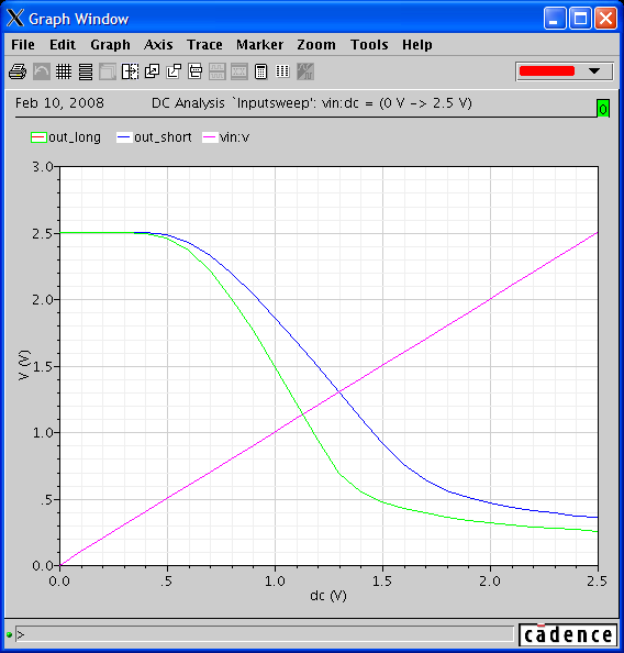
Here is the result of this simulation, shown in WaveScan.
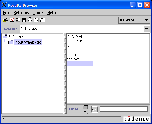
The window above was created by clicking in the result browser as shown below.
Tips for Exercise 5.5 (Source/Drain Sizes)
The source/drain extension and contact size information as specified in Question 5.5b relate to the physical sizes of the source and drain regions next to the channel. See for example color plate 5 and Figure 5.15 of the Rabaey book. These are the active areas next to a transistor gate (typically drawn green in a color plate).
These regions have a relatively high capacitance and often also a non-negligible resistance. This is the reason that they need to be included in the simulation, if a good accuracy is required. (Of course, the C will only be relevant for the timing, not for the static properties.)
To include the source/drain effects in the simulation, you can add
parameters to the Spectre line containing the transistors. These
parameters specify the size of the source and drain regions, as area
and perimeter. (See 'Junction Capacitances' in Sec. 3.3 of the Rabaey
book.) The parameters are as, ps, ad and pd, for
area/perimeter of source/drain, respectively. They are measured in
square meters and meters, respectively. You will typically add the
scalefactor 'p' for pico (10^-12), in which you can specify the amount
of square micrometers for the area and u for micro (10^-1), in which
case you can specify the length of the perimeter in micro meter.
For Question 5.5b you should use square source/drain areas for both
devices, dimensions are 5 lambda times 5 lambda. Lambda is the basic
size unit, for the book being equal to 0.125*10^-6 meter. This makes
ad/as equal to 0.39p and pd/ps equal to 1.88u. (Please check this,
remember from Sec. 3.3 that the part of the source/drain perimeter
next to the gate is not to be counted.)
Also see for example page 300 of the Spectre Circuit Simulator User Guide (Example Circuits) on Page 300 (pdf version of the document). It contains these lines:
m1 ( nq a vdd vdd ) p l=0.35u w=2.60u ad=1.90p pd=6.66u as=1.90p ps=6.66u
m2 ( vss a nq vss ) n l=0.35u w=1.10u ad=0.80p pd=3.66u as=0.80p ps=3.66u
Just see how the above model line includes the sizes of source and drain.