MSc thesis project proposal
Superconducting flip-chip interconnects by lithographic stencil printing
Background
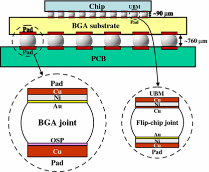
Quantum computers are increasingly recognized as a transformative technology with the potential to revolutionize fields ranging from cryptography and drug discovery to materials science and optimization problems. Superconducting qubits have demonstrated the ability to achieve high-fidelity quantum operations and control, meaning they can perform quantum gates and measurements with a high degree of accuracy and reliability. This is essential for building fault-tolerant quantum systems capable of running complex algorithms without significant errors. However, as the number of qubits increases, the likelihood of encountering issues with Josephson junctions in superconducting qubits also grows. Therefore, the next generation of quantum computers requires a multi-chip integration approach similar to that used in high-end conventional computing hardware. In conventional systems, multiple chips are combined into a single system using advanced packaging technologies, focusing on reliable, high-density electrical and mechanical interconnections between the chips. One key interconnect technology is the so-called flip-chip interconnect, where chips are connected face-to-face using Sn (tin) soldering, as illustrated in the figure
Flip-chip technology is mature and widely adopted, making it an excellent candidate for integrating multiple quantum chips. However, quantum chips operate at extremely low temperatures, and their interconnects must be superconducting. Although Sn is superconducting below 3.7 K, it becomes hard and brittle at cryogenic temperatures, which prevents the fabrication of mechanically stable and reliable interconnects.
For cryogenic applications, an alternative superconducting material, indium, is preferred due to its ductile nature and favourable thermal and electrical properties, and good superconducting performace at low temperatures. Several indium deposition techniques exist, such as sputtering, evaporation, and electroplating. Among these, electroplating is the preferred method for forming indium interconnects. However, this process requires intermediate metal films that are non-superconducting, potentially limiting overall performance.
In this project, we aim to develop a novel deposition and patterning method to fabricate indium flip-chip interconnect structures that will enable fully superconducting interconnects, enhancing the reliability and performance of quantum multi-chip systems.
Technology development
This project will explore the combined use of microlithography with stencil printing alongside the application of a novel indium-containing conductive paste.
Stencil printing is a deposition technique where a conductive paste is pressed through a stencil mask onto a substrate to form a patterned conductive layer. It is a widely used method for fabricating conductive patterns, particularly in conjunction with solder paste for creating interconnections. However, conventional stencil printing faces two major limitations in this context:
- The required feature size is smaller than the capabilities of traditional stencil printing.
- Conventional Sn-based solder pastes cannot be used
To achieve further downscaling, lithographic stencil printing is proposed. The key element in this approach is a high-resolution photolithographic photoresist pattern that serves as the stencil mask. Similar to conventional stencil printing, the photoresist film is removed at the end of the process, leaving behind a high-resolution conductive pattern on the substrate (see Figure 2). In addition, this project will apply a novel indium paste to replace tin-based materials with indium.
Several factors are critical to the success of this approach, including the rheology, viscosity, flowability, and adhesion properties of the novel indium paste. Furthermore, substrate characteristics and the choice of interconnect materials introduce additional parameters that require optimization. The properties of the photoresist itself are also significant, influencing the overall process. Optimization efforts will consider variables such as resist thickness, the selection between positive or negative photoresist, and the adhesion characteristics of the substrate.
Assignment
This master's thesis aims to explore and optimize key process parameters in lithographic stencil printing to achieve enhanced precision, efficiency, and quality in printed indium patterns. The study will investigate the impact of variables such as material properties, mask design, printing conditions, and post-processing techniques on the final printed interconnect. Finally, the high-resolution indium patterns will be integrated into a flip-chip interconnected device to characterize its electrical performance.
Project activities
- Conduct a literature study to assess the state of the art.
- Design a process flowchart for fabrication in the EKL cleanroom (DoE).
- Complete cleanroom process training.
- Design and fabricate relevant test structures.
- Select materials for substrates, photoresist, and the squeegee.
- Test candidate materials for flip-chip interconnects; determine compatibility and achievable patterning resolution.
- Optimize process parameters and fabricate devices.
- Perform electrical characterisation at relevant temperatures.
- Write the final report.
Contact information
Dr. Henk van Zeijl, h.w.vanzeijl@tudelft.nl
Dr. Nadia Haider, s.n.haider@tudelft.nl
Prof. Willem van Driel, willem.vandriel@tudelft.nl
Requirements
You are an ambitious, hands-on Master student with a background in (micro)electronics, material engineering or applied physics. You have an affinity for working in a multi-disciplinary context, including microfabrication, design and characterization of devices. You have good communication skills in English, you are independent and a team player.
Contact
prof.dr.ir. Willem van Driel
Electronic Components, Technology and Materials Group
Department of Microelectronics
Last modified: 2026-02-06