MSc thesis project proposal
Low-latency Interleaved SAR ADC (NXP)
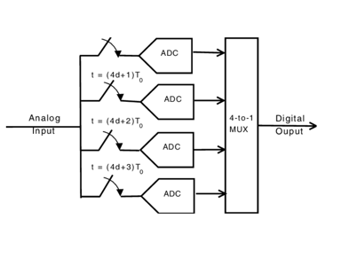
In this project you will work on an interleaved Successive approximation (SAR) analog-to-digital converter architecture which can achieve broadband data conversion with low-latency. Traditionally, a time-interleaved ADC functions in a time-multiplex manner and its latency is defined by the throughput time of each ADC unit. In the first part of the thesis, you will investigate techniques such frequency and time interleaving. Later, the proposed architecture will be implemented by adapting the SAR converter which has been already tape-out in CMOS 28nm process [1].
In this master thesis project you will do/learn:
- In depth study of ADC (or DAC) architecture
- Design of analog and mixed-signal circuits in 28nm CMOS
- Circuit simulations with Spectre (or other simulator)
- Layout design of circuits and simulation of extracted layout
- Build understanding of impact of process imperfections and parasitic artifacts on performance
A stipend is provided.
Ref:
[1] P. Cenci et al., “A 3.2mW SAR-assisted CTΔΣ ADC with 77.5dB SNDR and 40MHz BW in 28nm CMOS,” in 2019 Symposium on VLSI Circuits, Jun. 2019, pp. C230–C231.
Assignment
Overview of the project planning (depending on the progress of the student):
- Literature review of the recent time and frequency interleaved data converters.
- System level study of the proposed ADC architecture in Matlab/Cadence.
- Circuit and layout implementation.
- Tape-out of the IC followed by measurement.
- Process node: 28nm HPCP.
- Target tape-out date: June 2025
Requirements
- Good knowledge of analog and mixed circuit design.
- Good understanding of Data Converters.
- Familiarity with Matlab and Cadence.
- You will be collaborating with researchers from NXP Semiconductors so good communication and presentation skills are essential.
Contact
dr.ir. Muhammed Bolatkale
Electronic Instrumentation Group
Department of Microelectronics
Last modified: 2026-02-02