EE4710 Solid state physics with quantum and nano electronics
In electrical engineering, solid-state materials play an essential role in many applications. When solids are reduced in the size to nanometer scale by nanofabrication, the quantum effect becomes evident, and they exhibit exciting behaviors. A thorough understanding of the basic quantum mechanics and electrical and physical properties of semiconductors, metals and insulators are essential for design and fabrication of novel nanoelectronic and photonic devices for the applications in classical and quantum computers, memories, displays, solar-cells, light emitting diodes, and sensors.
The course consists of two parts. The first part deals with solid-state physics; After introduction of IC fabrication process, the course starts with the crystallography and then will be followed by the quantum mechanics, the quantum theory of solid, semiconductor physics. In short, you will be acquainted with the properties of individual atoms and what happens when they meet and become the form of a solid.
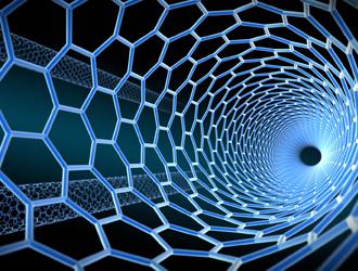
In the second part, we will discuss (1) properties of low-dimensional structures, with examples of nanomaterials such as graphene, (2) electric field transport in nanostructures, (3) the quantum Hall effect, (4) electrical and optical process in quantum wells and quantum dots, and (5) selected applications using the nanomaterial and nanostructures, such as, single-electron transistors and photonic crystals.
Study Goals
For the first part, the student can 1) determine the crystal structure, the density of atoms and the Miller indices of a crystal, 2) apply Schrodinger’s wave equation to various potential functions and derive a probability of finding electrons, 3) find the eigenvalues and eigenfunctions of the Hamiltonian of the system by perturbation methods, 4) discuss the concepts of energy band formation using nearly free electron model and tight-binding approximation, and difference of material properties in terms of the band, 5) derive the concentrations of electron and holes with a given temperature in terms of Fermi energy, and 6) can discuss drift, diffusion and scattering of carriers in a semiconductor under various temperature and impurity concentrations.
For the second part, the student can 1) analyze, explain and evaluate a specific application of an (nano)electronic or photonic device/material using the obtained knowledge, and 2) create idea for device(s)/material(s) beyond the state-of-the-art for a specific application.
Teachers
dr. Ryoichi Ishihara (ECTM)
Thin Film Transistors
Last modified: 2023-11-04
Details
| Credits: | 5 EC |
|---|---|
| Period: | 0/0/4/0 |